Vol. 3A 11-35
MEMORY CACHE CONTROL
11.12.3 Selecting a Memory Type from the PAT
To select a memory type for a page from the PAT, a 3-bit index made up of the PAT, PCD, and PWT bits must be
encoded in the page-table or page-directory entry for the page. Table 11-11 shows the possible encodings of the
PAT, PCD, and PWT bits and the PAT entry selected with each encoding. The PAT bit is bit 7 in page-table entries
that point to 4-KByte pages and bit 12 in paging-structure entries that point to larger pages. The PCD and PWT bits
are bits 4 and 3, respectively, in paging-structure entries that point to pages of any size.
The PAT entry selected for a page is used in conjunction with the MTRR setting for the region of physical memory
in which the page is mapped to determine the effective memory type for the page, as shown in Table 11-7.
11.12.4 Programming the PAT
Table 11-12 shows the default setting for each PAT entry following a power up or reset of the processor. The setting
remain unchanged following a soft reset (INIT reset).
The values in all the entries of the PAT can be changed by writing to the IA32_PAT MSR using the WRMSR instruc-
tion. The IA32_PAT MSR is read and write accessible (use of the RDMSR and WRMSR instructions, respectively) to
software operating at a CPL of 0. Table 11-10 shows the allowable encoding of the entries in the PAT. Attempting to
write an undefined memory type encoding into the PAT causes a general-protection (#GP) exception to be gener-
ated.
The operating system is responsible for insuring that changes to a PAT entry occur in a manner that maintains the
consistency of the processor caches and translation lookaside buffers (TLB). This is accomplished by following the
procedure as specified in Section 11.11.8, “MTRR Considerations in MP Systems,” for changing the value of an
MTRR in a multiple processor system. It requires a specific sequence of operations that includes flushing the
processors caches and TLBs.
The PAT allows any memory type to be specified in the page tables, and therefore it is possible to have a single
physical page mapped to two or more different linear addresses, each with different memory types. Intel does not
support this practice because it may lead to undefined operations that can result in a system failure. In particular,
a WC page must never be aliased to a cacheable page because WC writes may not check the processor caches.
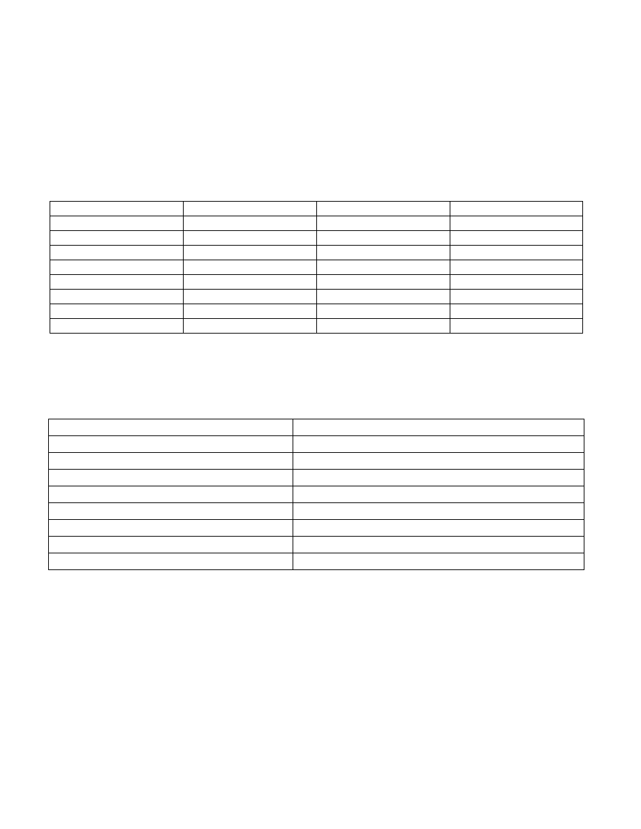
Table 11-11. Selection of PAT Entries with PAT, PCD, and PWT Flags
PAT
PCD
PWT
PAT Entry
0
0
0
PAT0
0
0
1
PAT1
0
1
0
PAT2
0
1
1
PAT3
1
0
0
PAT4
1
0
1
PAT5
1
1
0
PAT6
1
1
1
PAT7
Table 11-12. Memory Type Setting of PAT Entries Following a Power-up or Reset
PAT Entry
Memory Type Following Power-up or Reset
PAT0
WB
PAT1
WT
PAT2
UC-
PAT3
UC
PAT4
WB
PAT5
WT
PAT6
UC-
PAT7
UC