17-2 Vol. 3B
DEBUG, BRANCH PROFILE, TSC, AND RESOURCE MONITORING FEATURES
•
Execution of any instruction.
•
Execution of an instruction at a specified address.
•
Read or write to a specified memory address/range.
•
Write to a specified memory address/range.
•
Input from a specified I/O address/range.
•
Output to a specified I/O address/range.
•
Attempt to change the contents of a debug register.
17.2 DEBUG
REGISTERS
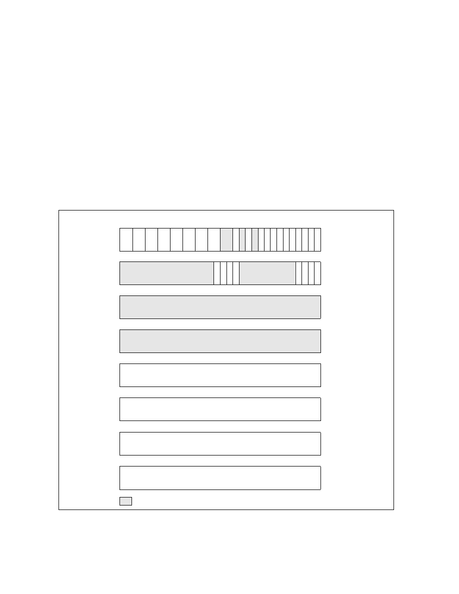
Eight debug registers (see Figure 17-1 for 32-bit operation and Figure 17-2 for 64-bit operation) control the debug
operation of the processor. These registers can be written to and read using the move to/from debug register form
of the MOV instruction. A debug register may be the source or destination operand for one of these instructions.
Figure 17-1. Debug Registers
31
24 23 22 21 20 19
16 15
13
14
12 11
8 7
0
DR7
L
Reserved
0
1
2
3
4
5
6
9
10
17
18
25
26
27
28
29
30
G
0
L
1
L
2
L
3
G
3
L
E
G
E
G
2
G
1
0 0
G
D
R/W
0
LEN
0
R/W
1
LEN
1
R/W
2
LEN
2
R/W
3
LEN
3
31
16 15
13
14
12 11
8 7
0
DR6
B
0
1
2
3
4
5
6
9
10
B
1
B
2
B
3
0 1 1 1 1 1 1 1 1
B
D
B
S
B
T
31
0
DR5
31
0
DR4
31
0
DR3
Breakpoint 3 Linear Address
31
0
DR2
Breakpoint 2 Linear Address
31
0
DR1
Breakpoint 1 Linear Address
31
0
DR0
Breakpoint 0 Linear Address
0
Reserved (set to 1)
1
R
T
M
R
T
M