Vol. 3A 12-5
INTEL
®
MMX
™
TECHNOLOGY SYSTEM PROGRAMMING
12.5.1
Effect of MMX Instructions on Pending x87 Floating-Point Exceptions
If an x87 FPU floating-point exception is pending and the processor encounters an MMX instruction, the processor
generates a x87 FPU floating-point error (#MF) prior to executing the MMX instruction, to allow the pending excep-
tion to be handled by the x87 FPU floating-point error exception handler. While this exception handler is executing,
the x87 FPU state is maintained and is visible to the handler. Upon returning from the exception handler, the MMX
instruction is executed, which will alter the x87 FPU state, as described in Section 12.2, “The MMX State and MMX
Register Aliasing.”
12.6 DEBUGGING
MMX
CODE
The debug facilities operate in the same manner when executing MMX instructions as when executing other IA-32
or Intel 64 architecture instructions.
To correctly interpret the contents of the MMX or x87 FPU registers from the FSAVE/FNSAVE or FXSAVE image in
memory, a debugger needs to take account of the relationship between the x87 FPU register’s logical locations
relative to TOS and the MMX register’s physical locations.
In the x87 FPU context, STn refers to an x87 FPU register at location n relative to the TOS. However, the tags in the
x87 FPU tag word are associated with the physical locations of the x87 FPU registers (R0 through R7). The MMX
registers always refer to the physical locations of the registers (with MM0 through MM7 being mapped to R0
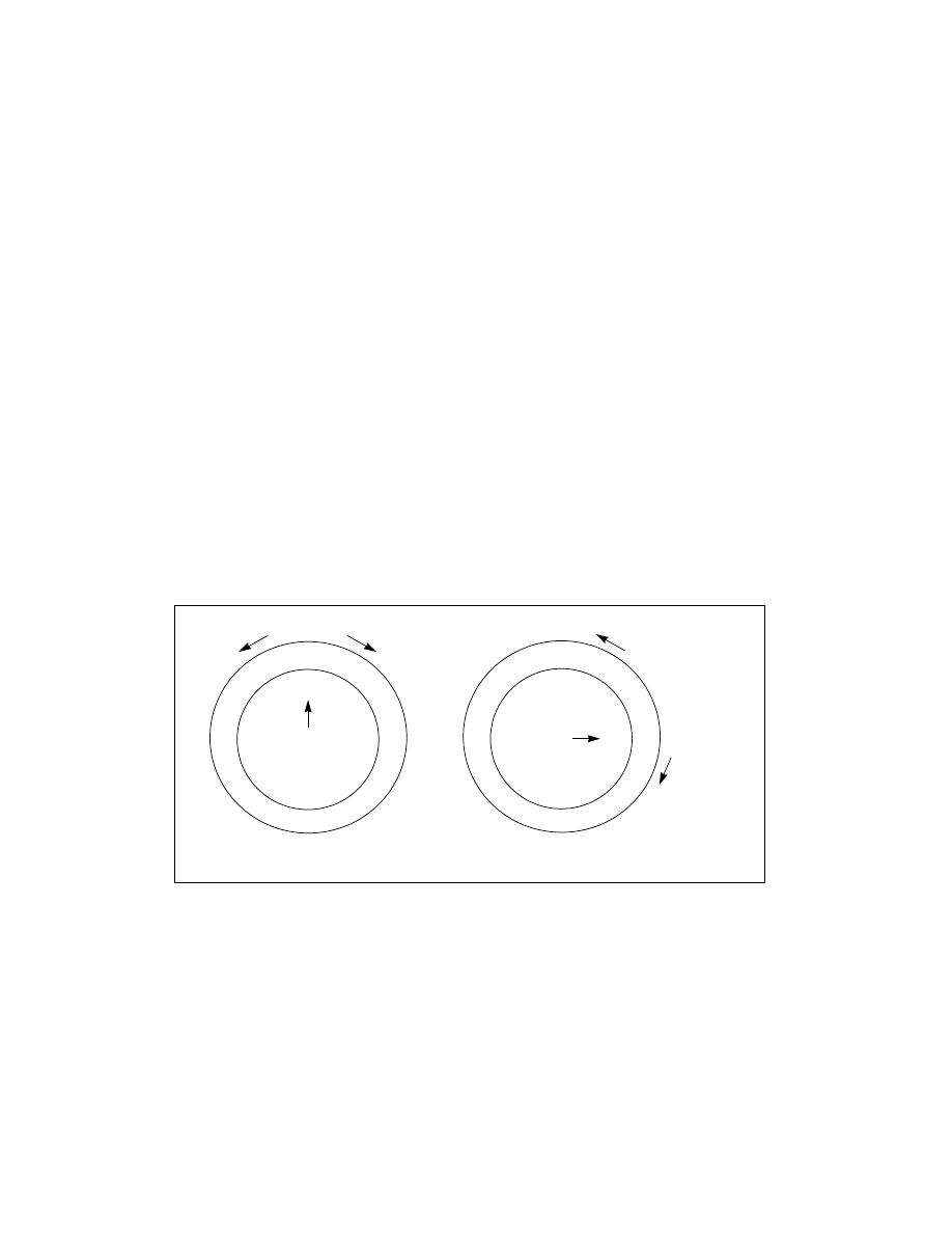
through R7). Figure 12-2 shows this relationship. Here, the inner circle refers to the physical location of the x87
FPU and MMX registers. The outer circle refers to the x87 FPU registers’s relative location to the current TOS.
When the TOS equals 0 (case A in Figure 12-2), ST0 points to the physical location R0 on the floating-point stack.
MM0 maps to ST0, MM1 maps to ST1, and so on.
When the TOS equals 2 (case B in Figure 12-2), ST0 points to the physical location R2. MM0 maps to ST6, MM1
maps to ST7, MM2 maps to ST0, and so on.
Figure 12-2. Mapping of MMX Registers to x87 FPU Data Register Stack
MM0
MM1
MM2
MM3
MM4
MM5
MM6
MM7
ST1
ST2
ST7
ST0
ST6
ST7
ST1
TOS
TOS
x87 FPU “push”
x87 FPU “pop”
x87 FPU “push”
x87 FPU “pop”
Case A: TOS=0
Case B: TOS=2
MM0
MM1
MM2
MM3
MM4
MM5
MM6
MM7
ST0
Outer circle = x87 FPU data register’s logical location relative to TOS
Inner circle = x87 FPU tags = MMX register’s location = FP registers’s physical location
(R0)
(R2)
(R2)
(R0)