Vol. 3A 12-1
CHAPTER 12
INTEL
®
MMX
™
TECHNOLOGY SYSTEM PROGRAMMING
This chapter describes those features of the Intel
®
MMX™ technology that must be considered when designing or
enhancing an operating system to support MMX technology. It covers MMX instruction set emulation, the MMX
state, aliasing of MMX registers, saving MMX state, task and context switching considerations, exception handling,
and debugging.
12.1
EMULATION OF THE MMX INSTRUCTION SET
The IA-32 or Intel 64 architecture does not support emulation of the MMX instructions, as it does for x87 FPU
instructions. The EM flag in control register CR0 (provided to invoke emulation of x87 FPU instructions) cannot be
used for MMX instruction emulation. If an MMX instruction is executed when the EM flag is set, an invalid opcode
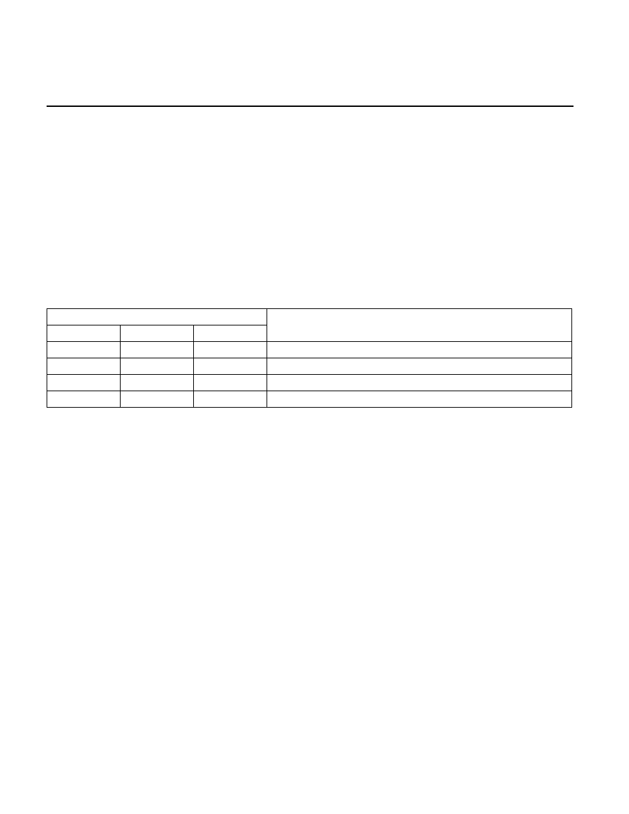
exception (UD#) is generated. Table 12-1 shows the interaction of the EM, MP, and TS flags in control register CR0
when executing MMX instructions.
12.2
THE MMX STATE AND MMX REGISTER ALIASING
The MMX state consists of eight 64-bit registers (MM0 through MM7). These registers are aliased to the low 64-bits
(bits 0 through 63) of floating-point registers R0 through R7 (see Figure 12-1). Note that the MMX registers are
mapped to the physical locations of the floating-point registers (R0 through R7), not to the relative locations of the
registers in the floating-point register stack (ST0 through ST7). As a result, the MMX register mapping is fixed and
is not affected by value in the Top Of Stack (TOS) field in the floating-point status word (bits 11 through 13).
Table 12-1. Action Taken By MMX Instructions for Different Combinations of EM, MP and TS
CR0 Flags
EM
MP*
TS
Action
0
1
0
Execute.
0
1
1
#NM exception.
1
1
0
#UD exception.
1
1
1
#UD exception.
NOTE:
* For processors that support the MMX instructions, the MP flag should be set.