11-26 Vol. 3A
MEMORY CACHE CONTROL
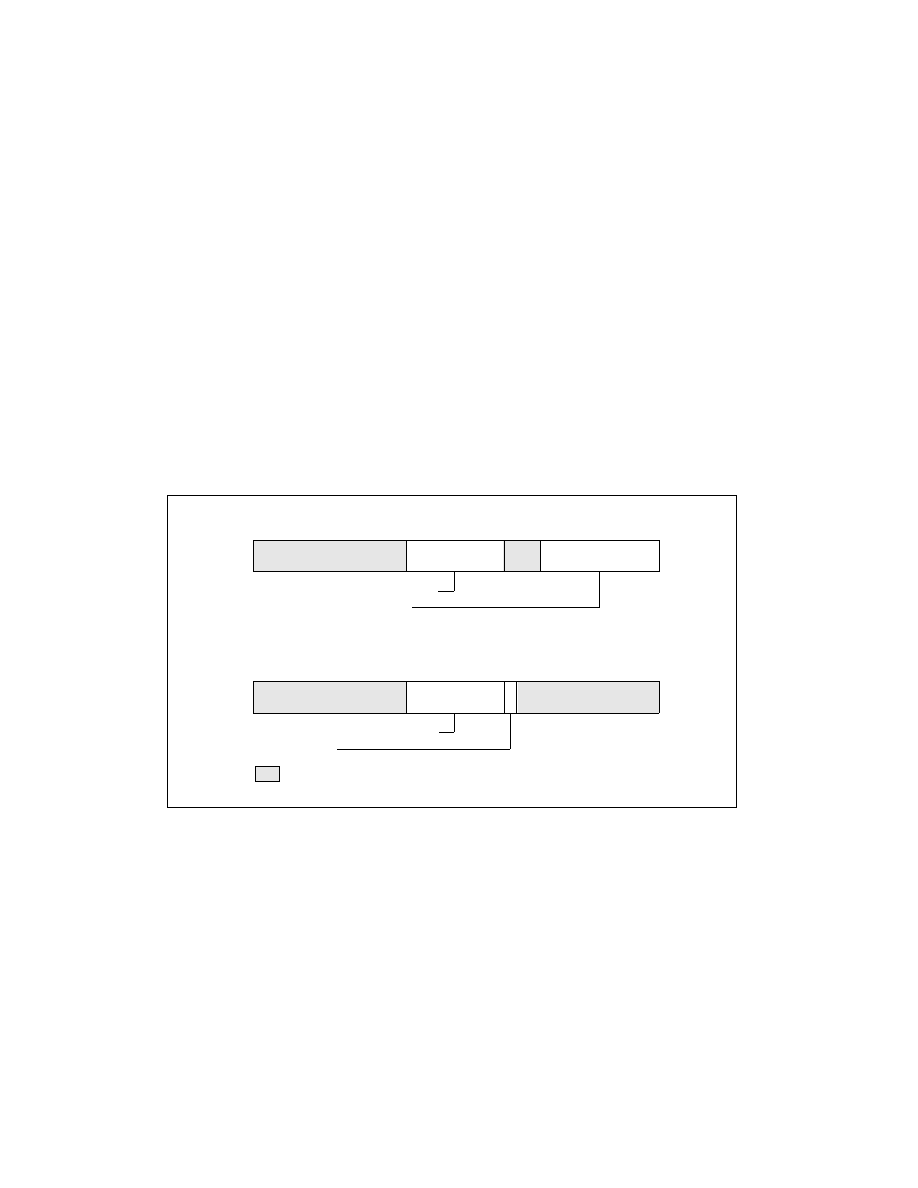
•
Type field, bits 0 through 7 — Specifies the memory type for the range (see Table 11-8 for the encoding of
this field).
•
PhysBase field, bits 12 through 31 — Specifies the base address of the address range. The address must be
less than 4 GBytes and is automatically aligned on a 4-KByte boundary.
•
PhysMask field, bits 12 through 31 — Specifies a mask that determines the range of the region being
mapped, according to the following relationships:
— Address_Within_Range AND PhysMask = PhysBase AND PhysMask
— This value is extended by 12 bits at the low end to form the mask value. For more information: see Section
11.11.3, “Example Base and Mask Calculations.”
•
V (valid) flag, bit 11 — Enables the register pair when set; disables register pair when clear.
Before attempting to access these SMRR registers, software must test bit 11 in the IA32_MTRRCAP register. If
SMRR is not supported, reads from or writes to registers cause general-protection exceptions.
When the valid flag in the IA32_SMRR_PHYSMASK MSR is 1, accesses to the specified address range are treated as
follows:
•
If the logical processor is in SMM, accesses uses the memory type in the IA32_SMRR_PHYSBASE MSR.
•
If the logical processor is not in SMM, write accesses are ignored and read accesses return a fixed value for each
byte. The uncacheable memory type (UC) is used in this case.
The above items apply even if the address range specified overlaps with a range specified by the MTRRs.
11.11.3 Example Base and Mask Calculations
The examples in this section apply to processors that support a maximum physical address size of 36 bits. The base
and mask values entered in variable-range MTRR pairs are 24-bit values that the processor extends to 36-bits.
For example, to enter a base address of 2 MBytes (200000H) in the IA32_MTRR_PHYSBASE3 register, the 12 least-
significant bits are truncated and the value 000200H is entered in the PhysBase field. The same operation must be
performed on mask values. For example, to map the address range from 200000H to 3FFFFFH (2 MBytes to 4
MBytes), a mask value of FFFE00000H is required. Again, the 12 least-significant bits of this mask value are trun-
cated, so that the value entered in the PhysMask field of IA32_MTRR_PHYSMASK3 is FFFE00H. This mask is chosen
so that when any address in the 200000H to 3FFFFFH range is AND’d with the mask value, it will return the same
value as when the base address is AND’d with the mask value (which is 200000H).
Figure 11-8. IA32_SMRR_PHYSBASE and IA32_SMRR_PHYSMASK SMRR Pair
V — Valid
PhysMask — Sets range mask
IA32_SMRR_PHYSMASK Register
63
0
Reserved
10
11
12
V
Reserved
31
PhysMask
Type — Memory type for range
PhysBase — Base address of range
IA32_SMRR_PHYSBASE Register
63
0
Reserved
11
12
Type
31
PhysBase
7
8
Reserved