11-16 Vol. 3A
MEMORY CACHE CONTROL
11.5.2.3 Writing Values Across Pages with Different Memory Types
If two adjoining pages in memory have different memory types, and a word or longer operand is written to a
memory location that crosses the page boundary between those two pages, the operand might be written to
memory twice. This action does not present a problem for writes to actual memory; however, if a device is mapped
the memory space assigned to the pages, the device might malfunction.
11.5.3 Preventing
Caching
To disable the L1, L2, and L3 caches after they have been enabled and have received cache fills, perform the
following steps:
1. Enter the no-fill cache mode. (Set the CD flag in control register CR0 to 1 and the NW flag to 0.
2. Flush all caches using the WBINVD instruction.
3. Disable the MTRRs and set the default memory type to uncached or set all MTRRs for the uncached memory
type (see the discussion of the discussion of the TYPE field and the E flag in Section 11.11.2.1,
“IA32_MTRR_DEF_TYPE MSR”).
The caches must be flushed (step 2) after the CD flag is set to insure system memory coherency. If the caches are
not flushed, cache hits on reads will still occur and data will be read from valid cache lines.
The intent of the three separate steps listed above address three distinct requirements: (i) discontinue new data
replacing existing data in the cache (ii) ensure data already in the cache are evicted to memory, (iii) ensure subse-
quent memory references observe UC memory type semantics. Different processor implementation of caching
control hardware may allow some variation of software implementation of these three requirements. See note
below.
NOTES
Setting the CD flag in control register CR0 modifies the processor’s caching behaviour as indicated
in Table 11-5, but setting the CD flag alone may not be sufficient across all processor families to
force the effective memory type for all physical memory to be UC nor does it force strict memory
ordering, due to hardware implementation variations across different processor families. To force
the UC memory type and strict memory ordering on all of physical memory, it is sufficient to either
program the MTRRs for all physical memory to be UC memory type or disable all MTRRs.
For the Pentium 4 and Intel Xeon processors, after the sequence of steps given above has been
executed, the cache lines containing the code between the end of the WBINVD instruction and
before the MTRRS have actually been disabled may be retained in the cache hierarchy. Here, to
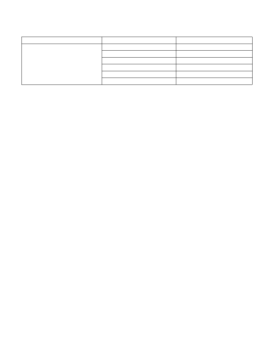
WP
UC
UC
2
UC-
WC
3
WC
WC
WT
WT
3
WB
WP
WP
WP
NOTES:
1. The UC attribute comes from the MTRRs and the processors are not required to snoop their caches since the data could never have
been cached. This attribute is preferred for performance reasons.
2. The UC attribute came from the page-table or page-directory entry and processors are required to check their caches because the
data may be cached due to page aliasing, which is not recommended.
3. These combinations were specified as “undefined” in previous editions of the Intel® 64 and IA-32 Architectures Software Devel-
oper’s Manual. However, all processors that support both the PAT and the MTRRs determine the effective page-level memory
types for these combinations as given.
Table 11-7. Effective Page-Level Memory Types for Pentium III and More Recent Processor Families (Contd.)
MTRR Memory Type
PAT Entry Value
Effective Memory Type