Vol. 3B 22-29
ARCHITECTURE COMPATIBILITY
22.29 CACHE
MANAGEMENT
The P6 family processors include two levels of internal caches: L1 (level 1) and L2 (level 2). The L1 cache is divided
into an instruction cache and a data cache; the L2 cache is a general-purpose cache. See Section 11.1, “Internal
Caches, TLBs, and Buffers,” for a description of these caches. (Note that although the Pentium II processor L2
cache is physically located on a separate chip in the cassette, it is considered an internal cache.)
The Pentium processor includes separate level 1 instruction and data caches. The data cache supports a writeback
(or alternatively write-through, on a line by line basis) policy for memory updates.
The Intel486 processor includes a single level 1 cache for both instructions and data.
The meaning of the CD and NW flags in control register CR0 have been redefined for the P6 family and Pentium
processors. For these processors, the recommended value (00B) enables writeback for the data cache of the
Pentium processor and for the L1 data cache and L2 cache of the P6 family processors. In the Intel486 processor,
setting these flags to (00B) enables write-through for the cache.
External system hardware can force the Pentium processor to disable caching or to use the write-through cache
policy should that be required. In the P6 family processors, the MTRRs can be used to override the CD and NW flags
(see Table 11-6).
The P6 family and Pentium processors support page-level cache management in the same manner as the Intel486
processor by using the PCD and PWT flags in control register CR3, the page-directory entries, and the page-table
entries. The Intel486 processor, however, is not affected by the state of the PWT flag since the internal cache of the
Intel486 processor is a write-through cache.
22.29.1 Self-Modifying Code with Cache Enabled
On the Intel486 processor, a write to an instruction in the cache will modify it in both the cache and memory. If the
instruction was prefetched before the write, however, the old version of the instruction could be the one executed.
To prevent this problem, it is necessary to flush the instruction prefetch unit of the Intel486 processor by coding a
jump instruction immediately after any write that modifies an instruction. The P6 family and Pentium processors,
however, check whether a write may modify an instruction that has been prefetched for execution. This check is
based on the linear address of the instruction. If the linear address of an instruction is found to be present in the
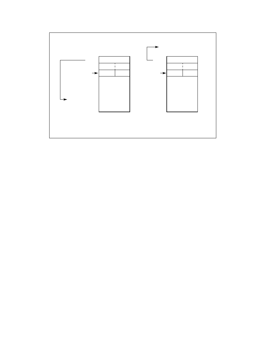
Figure 22-1. I/O Map Base Address Differences
Intel486 Processor
FFFFH
I/O Map
Base Addres
FFFFH
FFFFH + 10H = FH
for I/O Validation
0H
FFFFH
FFFFH
I/O access at port 10H checks
0H
FFFFH + 10H = Outside Segment
for I/O Validation
bitmap at I/O address FFFFH + 10H,
which exceeds segment limit.
Wrap around does not occur,
general-protection exception (#GP)
I/O access at port 10H checks
bitmap at I/O map base address
FFFFH + 10H = offset 10H.
Offset FH from beginning of
TSS segment results because
P6 family and Pentium Processors
I/O Map
Base Addres
occurs.
wraparound occurs.