Vol. 3A 11-1
CHAPTER 11
MEMORY CACHE CONTROL
This chapter describes the memory cache and cache control mechanisms, the TLBs, and the store buffer in Intel 64
and IA-32 processors. It also describes the memory type range registers (MTRRs) introduced in the P6 family
processors and how they are used to control caching of physical memory locations.
11.1
INTERNAL CACHES, TLBS, AND BUFFERS
The Intel 64 and IA-32 architectures support cache, translation look aside buffers (TLBs), and a store buffer for
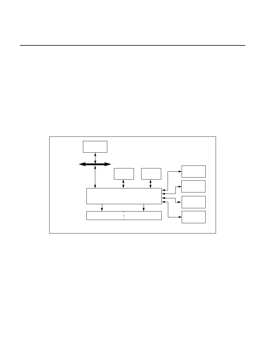
temporary on-chip (and external) storage of instructions and data. (Figure 11-1 shows the arrangement of caches,
TLBs, and the store buffer for the Pentium 4 and Intel Xeon processors.) Table 11-1 shows the characteristics of
these caches and buffers for the Pentium 4, Intel Xeon, P6 family, and Pentium processors. The sizes and char-
acteristics of these units are machine specific and may change in future versions of the processor. The
CPUID instruction returns the sizes and characteristics of the caches and buffers for the processor on which the
instruction is executed. See “CPUID—CPU Identification” in Chapter 3, “Instruction Set Reference, A-L,” of the
Intel® 64 and IA-32 Architectures Software Developer’s Manual, Volume 2A.
Figure 11-1. Cache Structure of the Pentium 4 and Intel Xeon Processors
Trace Cache
Instruction Decoder
Bus Interface Unit
System Bus
Data Cache
Unit (L1)
(External)
Physical
Memory
Store Buffer
Data TLBs
L2 Cache
Instruction
TLBs
L3 Cache
‚ÄÝ
‚ÄÝ Intel Xeon processors only