Vol. 3A 11-9
MEMORY CACHE CONTROL
Software can use page-level cache control, to assign appropriate effective memory types when software will not
access data structures in ways that benefit from write-back caching. For example, software may read a large data
structure once and not access the structure again until the structure is rewritten by another agent. Such a large
data structure should be marked as uncacheable, or reading it will evict cached lines that the processor will be
referencing again.
A similar example would be a write-only data structure that is written to (to export the data to another agent), but
never read by software. Such a structure can be marked as uncacheable, because software never reads the values
that it writes (though as uncacheable memory, it will be written using partial writes, while as write-back memory,
it will be written using line writes, which may not occur until the other agent reads the structure and triggers
implicit write-backs).
On the Pentium III, Pentium 4, and more recent processors, new instructions are provided that give software
greater control over the caching, prefetching, and the write-back characteristics of data. These instructions allow
software to use weakly ordered or processor ordered memory types to improve processor performance, but when
necessary to force strong ordering on memory reads and/or writes. They also allow software greater control over
the caching of data. For a description of these instructions and there intended use, see Section 11.5.5, “Cache
Management Instructions.”
11.3.3
Code Fetches in Uncacheable Memory
Programs may execute code from uncacheable (UC) memory, but the implications are different from accessing
data in UC memory. When doing code fetches, the processor never transitions from cacheable code to UC code
speculatively. It also never speculatively fetches branch targets that result in UC code.
The processor may fetch the same UC cache line multiple times in order to decode an instruction once. It may
decode consecutive UC instructions in a cacheline without fetching between each instruction. It may also fetch
additional cachelines from the same or a consecutive 4-KByte page in order to decode one non-speculative UC
instruction (this can be true even when the instruction is contained fully in one line).
Because of the above and because cacheline sizes may change in future processors, software should avoid placing
memory-mapped I/O with read side effects in the same page or in a subsequent page used to execute UC code.
11.4
CACHE CONTROL PROTOCOL
The following section describes the cache control protocol currently defined for the Intel 64 and IA-32 architec-
tures.
In the L1 data cache and in the L2/L3 unified caches, the MESI (modified, exclusive, shared, invalid) cache protocol
maintains consistency with caches of other processors. The L1 data cache and the L2/L3 unified caches have two
MESI status flags per cache line. Each line can be marked as being in one of the states defined in Table 11-4. In
general, the operation of the MESI protocol is transparent to programs.
The L1 instruction cache in P6 family processors implements only the “SI” part of the MESI protocol, because the
instruction cache is not writable. The instruction cache monitors changes in the data cache to maintain consistency
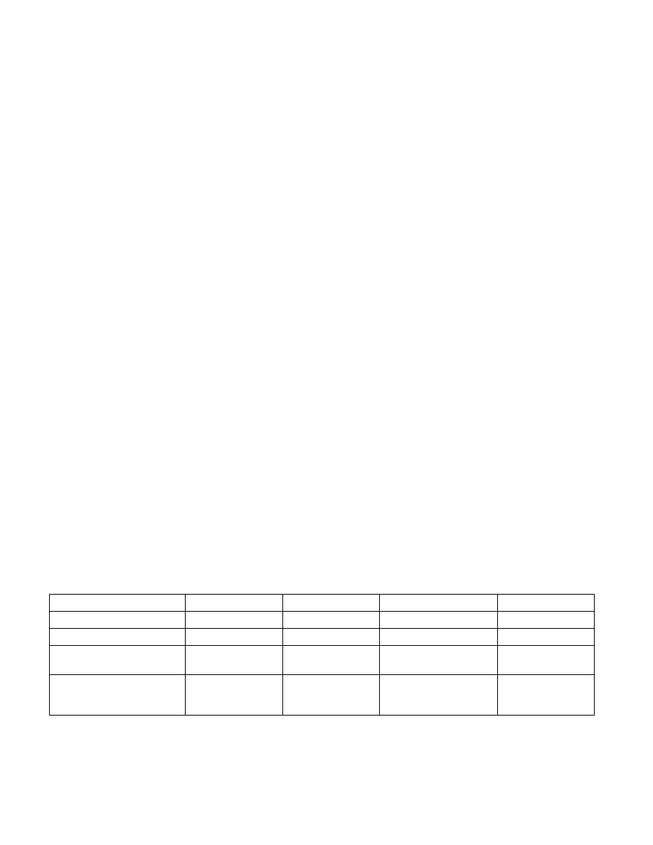
Table 11-4. MESI Cache Line States
Cache Line State
M (Modified)
E (Exclusive)
S (Shared)
I (Invalid)
This cache line is valid?
Yes
Yes
Yes
No
The memory copy is…
Out of date
Valid
Valid
—
Copies exist in caches of other
processors?
No
No
Maybe
Maybe
A write to this line …
Does not go to the
system bus.
Does not go to the
system bus.
Causes the processor to
gain exclusive ownership
of the line.
Goes directly to the
system bus.