11-4 Vol. 3A
MEMORY CACHE CONTROL
Intel 64 and IA-32 processors may implement four types of caches: the trace cache, the level 1 (L1) cache, the
level 2 (L2) cache, and the level 3 (L3) cache. See Figure 11-1. Cache availability is described below:
•
Intel Core i7, i5, i3 processor Family and Intel Xeon processor Family based on Intel
®
microarchi-
tecture code name Nehalem and Intel
®
microarchitecture code name Westmere — The L1 cache is
divided into two sections: one section is dedicated to caching instructions (pre-decoded instructions) and the
other caches data. The L2 cache is a unified data and instruction cache. Each processor core has its own L1 and
L2. The L3 cache is an inclusive, unified data and instruction cache, shared by all processor cores inside a
physical package. No trace cache is implemented.
•
Intel
®
Core™ 2 processor family and Intel
®
Xeon
®
processor family based on Intel
®
Core™ microar-
chitecture — The L1 cache is divided into two sections: one section is dedicated to caching instructions (pre-
decoded instructions) and the other caches data. The L2 cache is a unified data and instruction cache located
on the processor chip; it is shared between two processor cores in a dual-core processor implementation.
Quad-core processors have two L2, each shared by two processor cores. No trace cache is implemented.
•
Intel
®
Atom™ processor — The L1 cache is divided into two sections: one section is dedicated to caching
instructions (pre-decoded instructions) and the other caches data. The L2 cache is a unified data and
instruction cache is located on the processor chip. No trace cache is implemented.
•
Intel
®
Core™ Solo and Intel
®
Core™ Duo processors — The L1 cache is divided into two sections: one
section is dedicated to caching instructions (pre-decoded instructions) and the other caches data. The L2 cache
is a unified data and instruction cache located on the processor chip. It is shared between two processor cores
in a dual-core processor implementation. No trace cache is implemented.
•
Pentium
®
4 and Intel
®
Xeon
®
processors Based on Intel NetBurst
®
microarchitecture — The trace
cache caches decoded instructions (μops) from the instruction decoder and the L1 cache contains data. The L2
and L3 caches are unified data and instruction caches located on the processor chip. Dualcore processors have
two L2, one in each processor core. Note that the L3 cache is only implemented on some Intel Xeon processors.
•
P6 family processors — The L1 cache is divided into two sections: one dedicated to caching instructions (pre-
decoded instructions) and the other to caching data. The L2 cache is a unified data and instruction cache
located on the processor chip. P6 family processors do not implement a trace cache.
•
Pentium
®
processors — The L1 cache has the same structure as on P6 family processors. There is no trace
cache. The L2 cache is a unified data and instruction cache external to the processor chip on earlier Pentium
processors and implemented on the processor chip in later Pentium processors. For Pentium processors where
the L2 cache is external to the processor, access to the cache is through the system bus.
For Intel Core i7 processors and processors based on Intel Core, Intel Atom, and Intel NetBurst microarchitectures,
Intel Core Duo, Intel Core Solo and Pentium M processors, the cache lines for the L1 and L2 caches (and L3 caches
if supported) are 64 bytes wide. The processor always reads a cache line from system memory beginning on a 64-
byte boundary. (A 64-byte aligned cache line begins at an address with its 6 least-significant bits clear.) A cache
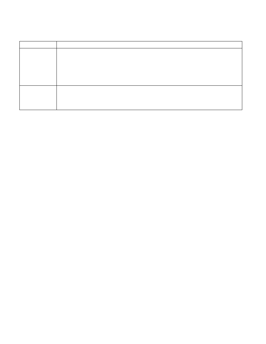
Store Buffer
• Intel Core i7, i5, i3 processors: 32entries.
• Intel Core 2 Duo processors: 20 entries.
• Intel Atom processors: 8 entries, used for both WC and store buffers.
• Pentium 4 and Intel Xeon processors: 24 entries.
• Pentium M processor: 16 entries.
• P6 family processors: 12 entries.
• Pentium processor: 2 buffers, 1 entry each (Pentium processors with MMX technology have 4 buffers for 4
entries).
Write Combining
(WC) Buffer
• Intel Core 2 Duo processors: 8 entries.
• Intel Atom processors: 8 entries, used for both WC and store buffers.
• Pentium 4 and Intel Xeon processors: 6 or 8 entries.
• Intel Core Duo, Intel Core Solo, Pentium M processors: 6 entries.
• P6 family processors: 4 entries.
NOTES:
1 Introduced to the IA-32 architecture in the Pentium 4 and Intel Xeon processors.
Table 11-1. Characteristics of the Caches, TLBs, Store Buffer, and
Write Combining Buffer in Intel 64 and IA-32 Processors (Contd.)
Cache or Buffer
Characteristics