Vol. 3A 11-11
MEMORY CACHE CONTROL
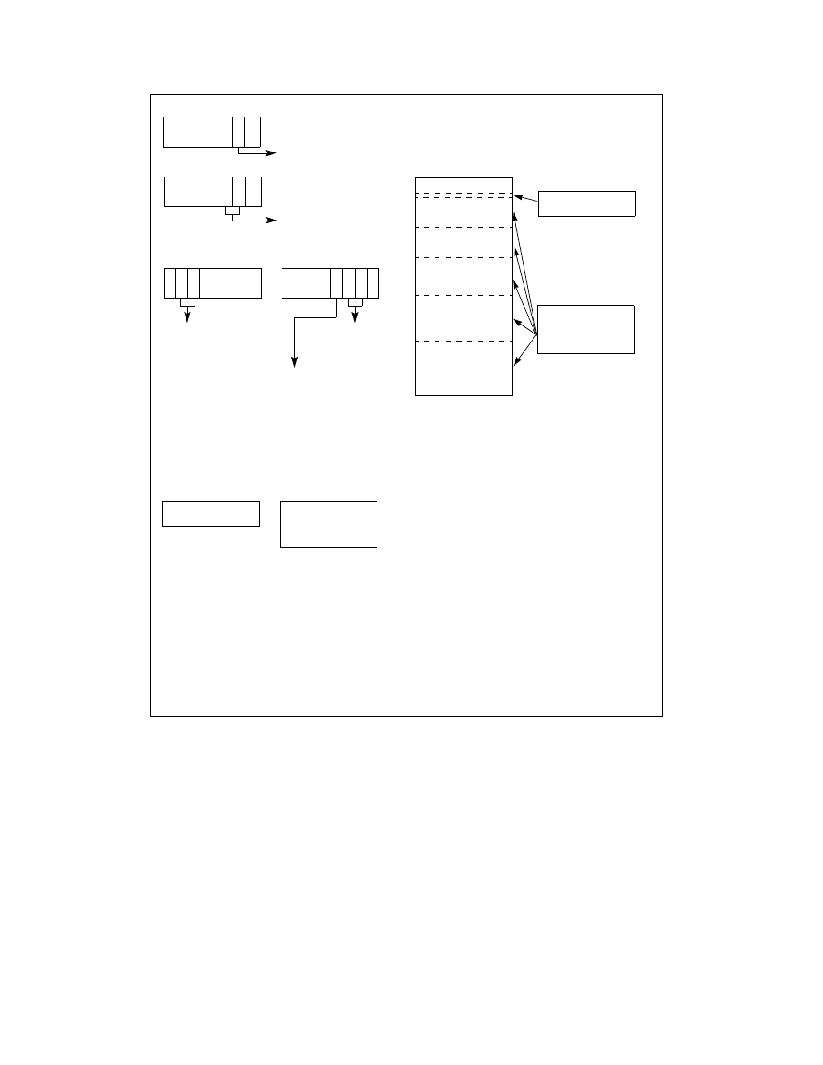
Figure 11-3. Cache-Control Registers and Bits Available in Intel 64 and IA-32 Processors
Page-Directory or
Page-Table Entry
TLBs
MTRRs
3
Physical Memory
0
FFFFFFFFH
2
control overall caching
of system memory
CD and NW Flags
PCD and PWT flags
control page-level
caching
G flag controls page-
level flushing of TLBs
MTRRs control caching
of selected regions of
physical memory
P
C
D
CR3
Control caching of
page directory
P
W
T
C
D
CR0
N
W
Store Buffer
P
C
D
P
W
T
G
1
CR4
Enables global pages
P
G
E
designated with G flag
1. G flag only available in P6 and later processor families
3. MTRRs available only in P6 and later processor families;
similar control available in Pentium processor with the KEN#
and WB/WT# pins.
2. The maximum physical address size is reported by CPUID leaf
function 80000008H. The maximum physical address size of
PAT
4
PAT controls caching
of virtual memory
pages
4. PAT available only in Pentium III and later processor families.
P
4
A
T
FFFFFFFFFH applies only If 36-bit physical addressing is used.
5. L3 in processors based on Intel NetBurst microarchitecture can
be disabled using IA32_MISC_ENABLE MSR.