35-324 Vol. 3C
MODEL-SPECIFIC REGISTERS (MSRS)
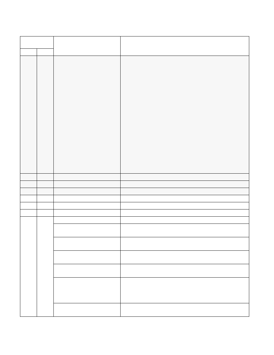
BBL_CR_CTL3[17:13
00001
00010
00100
01000
10000
BBL_CR_CTL3[12:11]
BBL_CR_CTL3[10:9]
00
01
10
11
BBL_CR_CTL3[8]
BBL_CR_CTL3[7]
BBL_CR_CTL3[6]
BBL_CR_CTL3[5]
BBL_CR_CTL3[4:1]
BBL_CR_CTL3[0]
Cache size per bank (read/write)
256KBytes
512KBytes
1MByte
2MByte
4MBytes
Number of L2 banks (read only)
L2 Associativity (read only)
Direct Mapped
2 Way
4 Way
Reserved
L2 Enabled (read/write)
CRTN Parity Check Enable (read/write)
Address Parity Check Enable (read/write)
ECC Check Enable (read/write)
L2 Cache Latency (read/write)
L2 Configured (read/write
)
174H
372
SYSENTER_CS_MSR
CS register target for CPL 0 code
175H
373
SYSENTER_ESP_MSR
Stack pointer for CPL 0 stack
176H
374
SYSENTER_EIP_MSR
CPL 0 code entry point
179H
377
MCG_CAP
17AH
378
MCG_STATUS
17BH
379
MCG_CTL
186H
390
PerfEvtSel0 (EVNTSEL0)
7:0
Event Select
Refer to Performance Counter section for a list of event encodings.
15:8
UMASK (Unit Mask)
Unit mask register set to 0 to enable all count options.
16
USER
Controls the counting of events at Privilege levels of 1, 2, and 3.
17
OS
Controls the counting of events at Privilege level of 0.
18
E
Occurrence/Duration Mode Select
1 = Occurrence
0 = Duration
19
PC
Enabled the signaling of performance counter overflow via BP0 pin
Table 35-46. MSRs in the P6 Family Processors (Contd.)
Register
Address
Register Name
Bit Description
Hex
Dec