Vol. 3C 35-323
MODEL-SPECIFIC REGISTERS (MSRS)
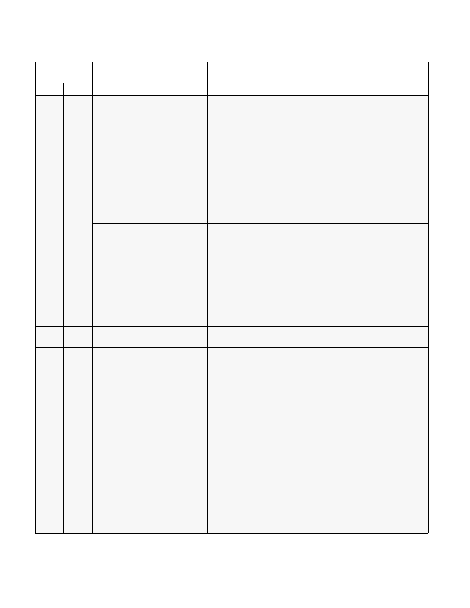
BBL_CR_CTL[20:19]
BBL_CR_CTL[18]
BBL_CR_CTL[17]
BBL_CR_CTL[16]
BBL_CR_CTL[15:14]
BBL_CR_CTL[13:12]
BBL_CR_CTL[11:10]
BBL_CR_CTL[9:8]
BBL_CR_CTL[7]
BBL_CR_CTL[6:5]
User supplied ECC
Reserved
L2 Hit
Reserved
State from L2
Modified - 11,Exclusive - 10, Shared - 01, Invalid - 00
Way from L2
Way 0 - 00, Way 1 - 01, Way 2 - 10, Way 3 - 11
Way to L2
Reserved
State to L2
BBL_CR_CTL[4:0]
01100
01110
01111
00010
00011
010 + MESI encode
111 + MESI encode
100 + MESI encode
L2 Command
Data Read w/ LRU update (RLU)
Tag Read w/ Data Read (TRR)
Tag Inquire (TI)
L2 Control Register Read (CR)
L2 Control Register Write (CW)
Tag Write w/ Data Read (TWR)
Tag Write w/ Data Write (TWW)
Tag Write (TW)
11AH 282
BBL_CR_TRIG
Trigger register: used to initiate a cache configuration accesses access,
Write only with Data = 0.
11BH 283
BBL_CR_BUSY
Busy register: indicates when a cache configuration accesses L2 command
is in progress. D[0] = 1 = BUSY
11EH
286
BBL_CR_CTL3
BBL_CR_CTL3[63:26]
BBL_CR_CTL3[25]
BBL_CR_CTL3[24]
BBL_CR_CTL3[23]
Control register 3: used to configure the L2 Cache
Reserved
Cache bus fraction (read only)
Reserved
L2 Hardware Disable (read only)
BBL_CR_CTL3[22:20]
111
110
101
100
011
010
001
000
BBL_CR_CTL3[19]
BBL_CR_CTL3[18]
L2 Physical Address Range support
64GBytes
32GBytes
16GBytes
8GBytes
4GBytes
2GBytes
1GBytes
512MBytes
Reserved
Cache State error checking enable (read/write)
Table 35-46. MSRs in the P6 Family Processors (Contd.)
Register
Address
Register Name
Bit Description
Hex
Dec